I got my hands on a broken Specialized TCU. The TCU is the controller of a Specialized e-bike, and this one is from a 2020/2021 Levo model. That means the device I looked at does not feature a touch screen. In this blog post I reverse engineer the TCU hardware and test whether the STM32 can be dumped. It turns out that the specific STM32 model is vulnerable to a well-known attack that abuses left-over state after a reboot and makes it possible to dump the flash contents.
The goal here is to learn more about Specialized e-bikes, how to diagnose problems with their electronics and how to actually repair them. It is sad to see that technical information is only available to authorized workshops. It is common to get diagnostic data from your car via a CAN bus, so why should this not be possible with an e-bike that can be more expensive than your car?
TCU
The TCU connects to the following components:
- Specialized Studio, a desktop app, via USB,
- the Specialized iOS/Android app via Bluetooth,
- TCD devices via ANT+,
- Remote on the handlebar via CAN,
- the motor via CAN,
- the battery via CAN,
- and optionally e-bike lights via CAN.
I was also able to find the TCU in the FCC database. This database is really helpful, as it shows internal pictures as well as technical schematics and information about the SoCs used, before you even have to touch a device. Here are some internal pictures of the TCU. Sometimes you can even find the names of PCB pads or removed debugging connectors.
The TCU uses an STM32F105, one of the older revisions of the STM32F1 family. The STM32 offers flash protection, which was enabled on this device. The mechanism is called readout protection (RDP) and is documented here. If I remember correctly, level 2 was set; however, it has been a while since I checked, so maybe I just assumed it was level 2.
Reading the flash with RDP enabled
In 2017, Johannes Obermaier and Stefan Tatschner found multiple weaknesses in the STM32. In 2020 they released another paper alongside a proof-of-concept (search for H3 in the paper).
The idea of the attack is based on the Flash Patch and Breakpoint Unit (FPB), which allows for live-patching during debugging. Typically, if the STM32 is in RDP mode 1 or 2, the flash memory is locked down. That means if you connect to the TCU via a debugger you cannot read the flash.
The attack then proceeds as follows:
- Upload the stage0 and stage1 exploit firmware to SRAM.
- Configure the STM32 to boot from SRAM via the BOOT pins.
- Reboot the STM32 by power cycling it. This releases the flash-readout lock, and because the reboot is short enough the SRAM data stays intact.
- The stage0 firmware configures the FPB to boot stage1 next.
- Set the BOOT pins to boot from flash. Because of the FPB, the STM32 boots stage1 instead.
- The stage1 firmware dumps the flash contents via UART.
Stage1 is required because, even though the lock is released after the first reboot, you still cannot access the flash when booted from SRAM.
Proof-of-concept
The authors provide a full proof-of-concept at CTXz/stm32f1-picopwner. All you need is an ST-Link and a Pi Pico. The ST-Link is used to talk to the STM32 via the debugging port, while the Pi Pico takes care of restarting the chip and of the serial communication. When building the exploit firmware, you need to use the variant that sends data via USART3_TX.
The following pictures and tables describe which pads on the PCB map to which pins of the STM32. They also show how to connect everything, based on the README of the proof-of-concept.
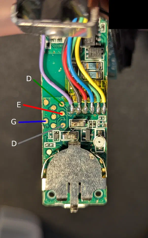
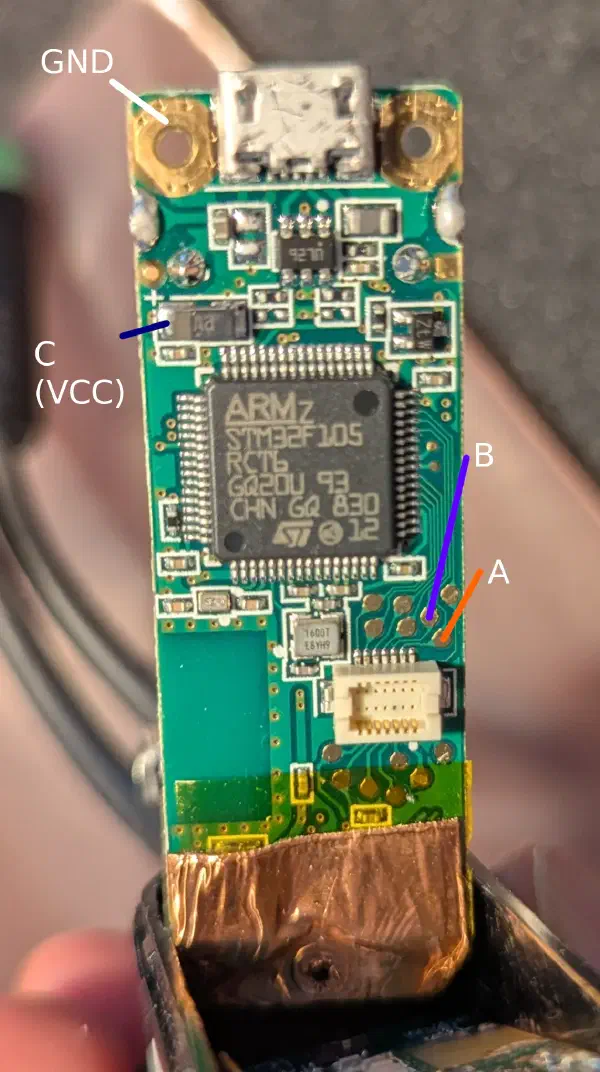
| TCU (STM32) | Pi Pico |
|---|---|
| A (USART3_TX) | Pin 2 (UART0 RX) |
| C (VDD) | Pin 4 (GPIO 2) |
| D (NRST) | Pin 6 (GPIO 4) |
| G (BOOT0) | Pin 7 (GPIO 5) |
B (BOOT1) is pulled up to VCC via a resistor. Make sure to connect the GND of the TCU (you can use the screw holes indicated in the picture).
Make sure to connect GND and VCC of the Pi Pico.
The STM32 will send out data via UART 3, so A is USART3_TX.
| TCU (STM32) | ST Link |
|---|---|
| E | TMS |
| F | CLK |
Make sure to connect GND and VCC of the ST-Link.
You may connect an LED to Pin 24 (GPIO 18) of the Pi Pico.
When executing the proof-of-concept you should see the flash data coming in. Dumping the chip takes about 5-15 minutes.
Conclusion
The most difficult part of this project was tracing the pads on the PCB to the pins of the STM32. I’m grateful for the detailed research by the authors of the paper: Johannes Obermaier, Marc Schink and Kosma Moczek.
This is only the first step, but it may allow us to diagnose Specialized e-bikes one day. Wouldn’t it be nice to check the cell health of your e-bike without taking a trip to an authorized Specialized workshop?